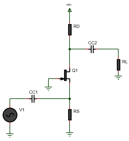
Common Source Gate Bias JFET Amplifier Calculator
Gate Biased JFET Calculator
The above JFET gate bias calculator helps to calculate the drain current \(I_D\), drain to source voltage \(V_{DS}\) from \(I_{DSS}\), \(V_{GS(off)}\), \(R_D\). In gate bias, a negative gate to source voltage is applied to the gate to reverse bias the gate to source junction of the JFET. The gate bias is also known as fixed bias. The gate bias method is usually used to bias the JFET in its ohmic region. It is not suitable for biasing the JFET in its active region due to variation of the JFET parameters. In ohmic region the JFET acts a resistor and a JFET biased with gate bias can be used as variable resistor controlled by the gate to source voltage. The tutorial JFET Gate Bias Circuit with Examples explains step by step the process of biasing a JFET with gate bias(fixed bias).
Equations Used:
\(\newline\) (1) \(V_{GS} = V_{GS(off)}(1 - \sqrt{\frac{I_D}{I_{DSS}}})\) \(\newline\) (2) \(R_D=\frac{V_{DD}-V_{DS}}{I_D}\) \(\newline\) (3) \(Z_i = R_G \space [as \space R_{GS} \space is \space very \space large]\) \(\newline\) (4) \(Z_o = R_D \space [assuming \space r_d >> R_D]\) \(\newline\) (5) \(CC_1 = \frac{10}{2\pi f Z_i}\) \(\newline\) (6) \(CC_2 = \frac{10}{2\pi f Z_o}\) \(\newline\)
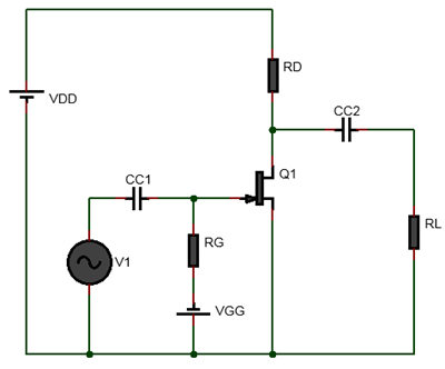
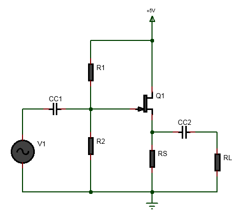
Common Source JFET Self Bias Amplifier Calculator
Self Bias JFET Amplifier Design Calculator
This self bias JFET amplifier design calculator helps you to bias a JFET using self biasing method. That is it helps to calculate the drain resistor value and the source resistor value. Furthermore it helps to calculate the coupling capacitors and bypass capacitor values. A detailed worked out example is shown in the tutorial self biased JFET amplifier design.Equations Used:
\(\newline\) (1) \(V_{GS}=\frac{V_{GS(off)}}{3.4}\)\(\newline\) (2) \(I_D = \frac{I_{DSS}}{2}\) \(\newline\) (3) \(R_S = \frac{V_{GS}}{I_D}\) \(\newline\) (4) \(R_D=\frac{V_{DD}-V_{D}}{I_{D}}\),\(\newline\) (5) \(g_m = \frac{2 I_{DSS}}{V_p} (1-\frac{V_{GS}}{V_p})\) \(\newline\) (6) \(R_d = R_D||R_L = \frac{R_DR_L}{R_D+R_L}\) \(\newline\) (7) \(A_v = -g_m R_d\) \(\newline\) (8) \(Z_i = R_G \space [as \space R_{GS} \space is \space very \space large]\) \(\newline\) (9) \(Z_o = R_D \space [Z_o=r_d||R_D\space assuming \space r_d >> R_D]\) \(\newline\) (10) \(CC_1 = \frac{10}{2\pi f Z_i}\) \(\newline\) (11) \(CC_2 = \frac{10}{2\pi f Z_o}\) \(\newline\)
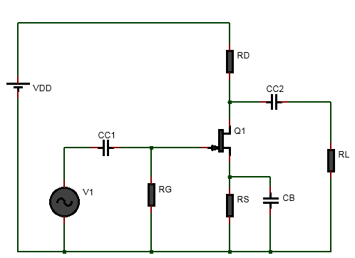
Voltage Divider Biased JFET Amplifier Calculator
About voltage divider biased JFET amplifier
The JFET voltage divider biasing calculator above calculates the biasing resistor values and coupling and by-pass capacitor values for given input and specification. This is helpful in quick determination for components values for designing JFET amplifiers. Voltage divider biasing is best suited for stable operation among the biasing methods. For detailed steps and explanations see JFET Biasing Worked Out Example CalculationEquations Used:
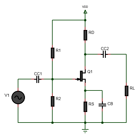
\(\newline\) (1) \(V_{GS} = \frac{V_{GS(off)}}{2}\) \(\newline\) (2) \(V_{G} = -V_{GS(off)}\) \(\newline\) (3) \(I_D=\frac{I_{DSS}}{4}\) \(\newline\) (4) \(R_{1}=R_2(\frac{V_{DD}}{V_{G}}-1) \space [assume \space R_2]\) \(\newline\) (5) \(V_{S}=\frac{V_G-V_{GS}}{I_D}\) \(\newline\) (6) \(R_S = \frac{V_S}{I_D}\) \(\newline\) (7) \(R_D = \frac{V_{DD}-V_D}{I_D} \space [assume \space V_D] \) \(\newline\) (8) \(r_d = R_D || R_L = \frac{R_D R_L}{R_D+R_L}\) \(\newline\) (9) \(g_m = \frac{2 I_{DSS}}{V_p} (1-\frac{V_{GS}}{V_p})\) \(\newline\) (10) \(A_v = g_m r_d\) \(\newline\) (11) \(Z_i = R_1 || R_2 || R_{GS} \approxeq R_1||R_2 \space [as \space R_{GS} \space is \space very \space large]\) \(\newline\) (12) \(Z_o = R_D \space \space[Z_o = r_d||R_D \space assuming \space r_d >> R_D] \) \(\newline\) (13) \(CC_1 = \frac{10}{2\pi f Z_i}\) \(\newline\) (14) \(CC_2 = \frac{10}{2\pi f Z_o}\) \(\newline\) (15) \(CB = \frac{10}{2\pi f R_S}\) \(\newline\)Common Drain JFET Amplifier Calculator
Equations Used:
\(\newline\) (1) \(V_{GS} = \frac{V_{GS(off)}}{2}\) \(\newline\) (2) \(V_{G} = -V_{GS(off)}\) \(\newline\) (3) \(I_D=\frac{I_{DSS}}{4}\) \(\newline\) (4) \(R_{1}=R_2(\frac{V_{DD}}{V_{G}}-1) \space [assume \space R_2]\) \(\newline\) (5) \(V_{S}=\frac{V_G-V_{GS}}{I_D}\) \(\newline\) (6) \(R_S = \frac{V_S}{I_D}\) \(\newline\) (7) \(r_s = R_S || R_L = \frac{R_S R_L}{R_S+R_L}\) \(\newline\) (8) \(g_m = \frac{2 I_{DSS}}{V_p} (1-\frac{V_{GS}}{V_p})\) \(\newline\) (9) \(A_v = \frac{g_m r_s}{1+g_m r_s}\) \(\newline\) (10) \(Z_i = R_1 || R_2\) \(\newline\) (11) \(Z_o = R_S||\frac{1}{g_m}\) \(\newline\) (12) \(CC_1 = \frac{10}{2\pi f Z_i}\) \(\newline\) (13) \(CC_2 = \frac{10}{2\pi f Z_o}\) \(\newline\)Common Gate JFET Amplifier Calculator