Mono Stable 555 Timer Calculator

The above figure shows 555 timer circuit diagram for monostable operation. In monostable operation, the 555 timer produces a square wave of pulse width of certain time duration(t) when there is trigger input signal at the trigger pin 2. The resistor R and the capacitor C are used here to control the pulse width of pulse duration(t) and is given by the following formula. \[t=1.1R_{}C_{}\] We can calculate the pulse width duration(t) using the above online 555 timer monostable calculator. For the trigger input we can connect a pulled high momentary push button to the trigger input pin 2. When we press the push button, there will be a square wave signal of width equal to the value obtained above.
Astable Multivibrator 555 Timer Calculator
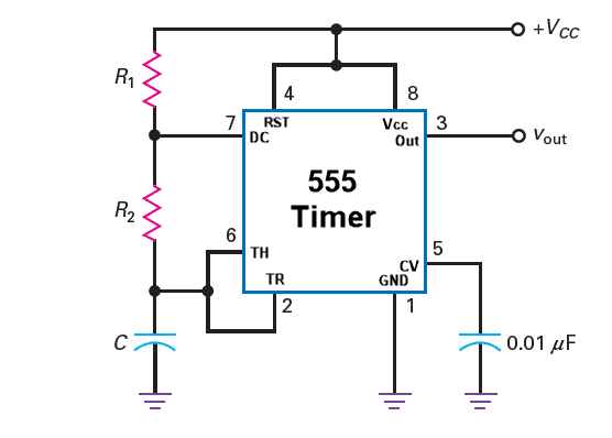
The above figure shows 555 timer circuit diagram for astable operation. Astable mode is also called Free Running Mode and the above circuit is often referred as free running non-sinusoidal oscillator. In astable operation, the threshold input is connected to the trigger input.
Formula Used \(T_{H}=0.693(R_{1}+R_{2})C,\newline T_{L}=0.693R_{2}C,\newline f=\frac{1.44}{(R_{1}+2R_{2})C},\newline DC=\frac{R_{1}+R_{2}}{R_{1}+2R_{2}}\)
Working Principle At start up, the dc power Vcc is turned on and when this happens the capacitor C is discharged and holds the trigger voltage less than 1/3rd of Vcc. This will trigger the internal comparator 2 which causes the output to switch from high and the internal discharge transistor Qd to turn off. When the internal discharge transistor Qd turns off, the external capacitor C will start to charge up via the resistors R1 and R2. When the voltage on capacitor C reaches 2/3rd of Vcc, the output switches low and internal discharge transistor Qd turns on. Now the capacitor C starts discharging via R2 and Qd. When the discharging operation reaches 1/3rd of Vcc the comparator 2 triggers causing the switch back to high and internal discharge transistor Qd is turned off. This cycle of charging and discharging repeats itself and the 555 Timer oscillates creating a square wave at the output pin 3.
